Soldermask Panels Specifications for Technosystem Loader/Unloader DI V3
This section focuses on the Soldermask Panels specifications and describes the criteria they need to meet for the correct functionality of the Technosystem Loader/Unloader DI V3
Soldermask Panel specifications for DI V3
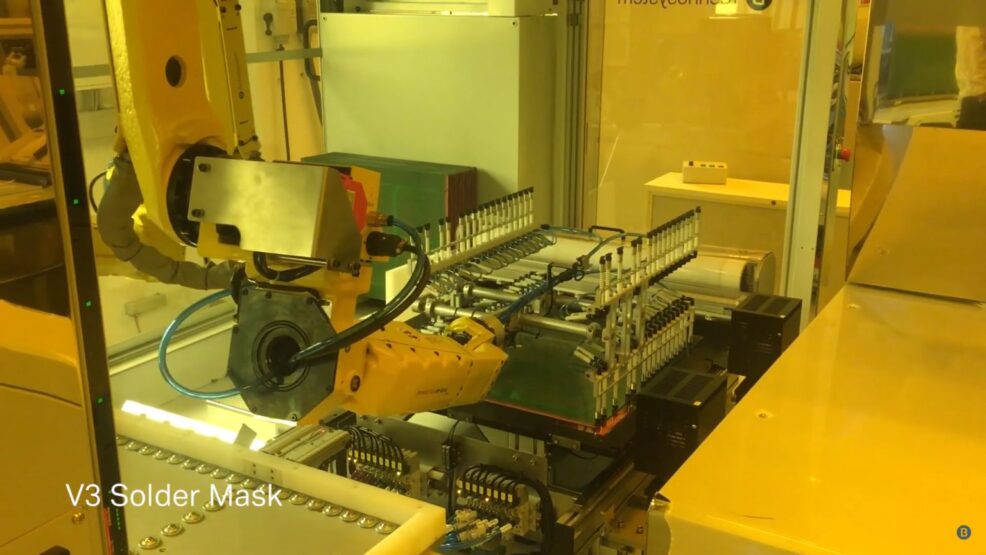
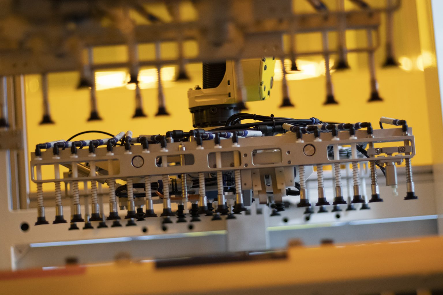
Technosystem Loader/Unloader DI V3 loads Soldermask panels from Slotted Racks and Dry Film panels from L Racks.
Both the Soldermask and the Dry Film panels need to be the same size for the DI V-III Loader good functionality. This because different panel sizes have to go respectively on different Slotted and L Racks.
Moreover, for the correct functionality of the Technosystem DI V-III, Soldermask panels need to have the following specifications:
- First, they need to be properly cut with a CNC routing machine.
- Second, the panel edge must be cut straight with a maximum deviation of +- 0,05º and must align 90º to the opposite axis.
- Finally, panels must be flat with a maximum warpage of 0,2% According to IPC standards*.
*Flatness requirements are very important to avoid loading problems
Soldermask Panels orientation specifications for DI V3
Loader/Unloader DI V3 loads Soldermask panels horizontally on the slotted racks (it is important to insert the long part of the panel into the slot).
Panel orientation on Slotted Racks in Nuvogo / Paragon / Express / Diamond and Ledia
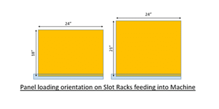
With respect to Solder mask panels, the system is only able to accommodate panels wider than 545mm in width*.
*Panels with smaller size than 545mm in x and y will require a special execution, please discuss it with Technosystem engineers.
Slotted Rack capacity specifications for DI V3
According to the customer requirements, every Slotted Rack can have 25 or 50 Slots.
Once the full Slotted rack is finished (side A+B) the loader will unload the Rack and enter a new one.
Panel non-useable area specifications
On solder mask panels where the non-useable area is less than 25mm from the edge of the panel, the suction cups will be in contact with functional areas of the PCB.
- Maximum thickness 2mm with a maximum copper thickness of 105 microns on the external layers.
- Minimum thickness 50-micron dielectric + copper on 2 sides. Flexible material (PI) coming from rolls excluded. For Flexible material (PI) the option, loading from horizontal boxes, needs to be implemented ( optional).
* Please discuss Other thickness with Technosystem Engineers